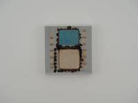
This is not a fragile consumer component. It feels like a piece of structural architecture. The massive ceramic substrate is cast in a deep, raw umber tone that is incredibly thick and practically bulletproof. Looking closely at the top surface, I immediately notice the eight massive bare silicon dies. The four central rectangular dies arranged in a cross are the primary processing cores. The four lighter, iridescent green square dies occupying the outer corners are the massive off-chip caches.
The micro-contrast on the dark mirror finish of the CPU dies reveals extremely faint laser etching, catching the light only at very specific angles. Meticulous clusters of tiny decoupling capacitors are brazed onto the ceramic around the perimeter of the dies with mechanical precision. Turning this specific artifact on its edge reveals pristine gold lettering stamped directly into the brown ceramic substrate.
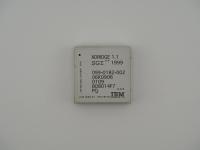
Edge Marking 1: FV783674
Edge Marking 2: FW666418
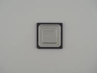
Flipping it over exposes the contact interface, and it is a masterpiece of high-end engineering. The massive Land Grid Array features over 5,000 individual gold pads. These are segmented perfectly into four isolated quadrants. The gold catches the light beautifully, showing zero signs of physical wear or bending.
The POWER5+ architecture represents IBM flexing its enterprise muscle to absolute extremes. By migrating from the 130nm process of the original POWER5 down to a 90nm fabrication node, IBM engineers managed to squeeze out higher clock speeds while aggressively reining in the thermal load.
Each of the four central processor dies houses two active cores. This gives us an 8-way symmetric multiprocessing behemoth residing on a single physical package. The four iridescent corner dies are dedicated L3 Cache modules. Each cache die holds 36MB, bringing the total L3 cache on this single slab to a staggering 144MB. The internal routing inside the thick ceramic layers connects these external caches to the compute cores via a proprietary Core Interface Unit, enabling insane bandwidths to keep the logic units fed. To deal with the massive heat density of eight bare dies running in close proximity, this package would have been bolted down under a massive liquid-cooled or heavily ducted copper block.
This exact slab of silicon was the beating heart of IBM's refrigerator-sized supercomputers and enterprise UNIX servers like the System p5 590 and 595. There is a running joke in the mainframe collector community that dropping an IBM server CPU on your foot requires an immediate hospital visit. Examining the dense ceramic and physical weight of this specific unit, I can confidently state that is not a joke.
A common piece of hardware lore was that IBM's implementation of Simultaneous Multithreading (SMT) in the POWER5 generation was just a reactionary clone of Intel's Hyper-Threading. In reality, IBM's design was vastly more aggressive. The chip dynamically allocated execution units on the fly based on thread priority and workload bottlenecks, making it a drastically different beast than consumer x86 logic.
Visually separating this POWER 5+ with the POWER5 without booting the host system is notoriously difficult because IBM reused the exact same 95mm by 95mm ceramic package for both generations.
However, the central dual-core processor dies on the 90nm POWER5+ are approximately 243 square millimeters. This is noticeably smaller than the older 389 square millimeter dies used on the 130nm process. Looking closely at the proportion of bare silicon to the surrounding decoupling capacitors on this specific artifact, the die footprint aligns beautifully with the 90nm shrink. The edge codes FV783674 and FW666418 are internal IBM assembly trackers that are completely absent from public databooks, but the physical geometry of the silicon dies proves its identity as the highly refined Plus variant.