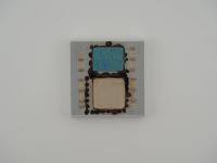

We have two distinct configurations here. The bare ceramic module weighs a substantial 52.9 grams, but when locked into its machined metal carrier assembly, the total weight jumps to a massive 458.7 grams. The substrate itself is a beautiful dark brown glass ceramic. The silicon die is completely exposed, acting as a mirror in the right light, surrounded by tiny surface mounted decoupling capacitors. As someone deeply drawn to intricate ceramic and gold engineering, inspecting this piece is an absolute masterclass in high-end fabrication.
Looking closely at the surface and utilizing the micro-contrast captured in these shots to read the laser etchings, I documented the following text across the artifact:
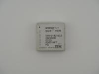
Module Edge Text (Gold Stamped): FM188772
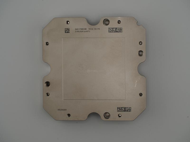
Carrier Top Text: G4C1T00C0B 9316 CA PQ
Carrier Top Text: SYA193P164971
Carrier Top Text: 45J0689
Surface SMD Components: H116 2FB 2
The underside of the ceramic features a phenomenally dense array of circular gold pads. The metal carrier frame is industrial art in its own right. This metal assembly acts as a protective retention bracket, ensuring the fragile ceramic does not crack under the immense pressure required to seat thousands of pins into the motherboard socket.
Diving into the technical weeds reveals why this processor requires such extreme packaging. Fabricated on a 45nm Silicon-On-Insulator process, the POWER7 silicon measures 567 square millimeters and packs roughly 1.2 billion transistors. IBM engineered this chip to house up to eight cores, with each core capable of four-way simultaneous multithreading. This massive parallelization results in 32 concurrent threads per socket.
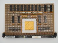
One of the most fascinating architectural quirks is the memory subsystem. Instead of traditional SRAM, IBM utilized eDRAM for the massive 32 MB L3 cache. This allowed them to pack significantly more cache capacity into a smaller die area while strictly managing leakage current. With a TDP hitting the 200-watt range depending on the specific clock configuration, this processor ran exceptionally hot. These thermal challenges dictate the physical design. The steel frame distributes the load from the massive copper heatsinks directly to the socket mechanism, protecting the bare silicon and allowing for maximum thermal transfer.
The legacy of the POWER7 architecture is permanently cemented in both server rooms and popular culture. This is the exact architecture that powered the IBM Watson supercomputer, famously defeating human champions on the television show Jeopardy in 2011.
Within hardware circles, POWER7 represents a massive philosophical pivot for IBM. Its predecessor, the POWER6, was designed purely for brute-force clock speed, hitting up to 5.0 GHz with an in-order execution pipeline. For POWER7, IBM shifted entirely toward parallel efficiency. They backed down the clock speeds to a maximum of 4.25 GHz and implemented an aggressive out-of-order execution engine. It is honestly quite funny to think that intentionally slowing down the clock is what actually crowned IBM as the king of enterprise parallel computing for a solid half decade. A common misconception about the POWER7 is that the naked, exposed silicon makes it delicate and prone to cracking in a high-stress server environment. In reality, the carrier mechanism protects the die flawlessly while enabling the direct metal-to-silicon contact necessary to keep the architecture from thermally throttling.
I am highly confident in this identification. The visual evidence directly points to an IBM Single Chip Module configuration built for the Power Systems family. The most conclusive piece of forensic data is the part number 45J0689 laser etched into the heavy metal carrier. Checking server maintenance logs and parts catalogs confirms this specific carrier assembly was utilized for POWER7 processors deployed in IBM Power 730 and Power 740 server enclosures.
The physical dimensions, the 45nm exposed die footprint, and the proprietary 2D matrix barcode format all perfectly match IBM fabrication standards from the early 2010s. The date code 9316 on the carrier likely indicates a specific manufacturing or assembly batch, but the broader architectural design clearly aligns with the 2010 rollout of the POWER7 generation.