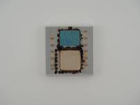
Holding this piece, the first thing I noticed was the satisfying density of the ceramic. At exactly 10.7 grams, it has a substantial feel for a chip measuring roughly 25mm by 35mm. The top features a flawless, matte silver metallic cap, likely an integrated heat spreader or a protective lid, bonded to a pristine white ceramic substrate.
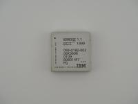
The laser etching on the cap is incredibly crisp, standing out with high micro-contrast against the metal. Here is the exact transcription of the surface text:
IBM
50G5741   P
304-01331-01
PLURIS STARFISH
IBM93 B4400252
Flipping this artifact over reveals a beautiful, high-density Ceramic Ball Grid Array. The solder balls are perfectly intact and tightly packed, with the corners naturally omitted to assist with orientation and stress relief during the reflow process. The small black orientation dot on the front cap perfectly aligns with the internal routing to pin 1. It is a stunning example of turn-of-the-millennium enterprise silicon packaging.
When examining a custom ASIC like this, we are looking at the bleeding edge of networking hardware from the height of the dot-com boom. IBM Microelectronics was an absolute juggernaut in the custom silicon foundry business during this era, leveraging their "Blue Logic" design methodology to help third-party companies spin up massive, highly complex chips.
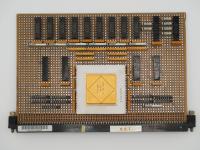
The Starfish ASIC was designed to be the brains of a massively parallel networking fabric. To handle terabits of data per second, these chips required immense I/O capabilities, which explains the dense BGA on the underside. The ceramic substrate is not just for show; it is an absolute necessity for thermal management. Routing massive amounts of internet traffic at wire speed generates a tremendous amount of heat, and the white ceramic paired with the metal lid ensured the silicon die underneath would not cook itself to death in a crowded telecom rack.
This chip is a literal fossil from the great dot-com extinction event. Pluris Inc. was a high-flying Silicon Valley startup founded in the late 1990s with a singular, incredibly ambitious goal: to build the world's largest, fastest internet core router. They wanted to dethrone Cisco and Juniper with their "Teraplex" systems, which promised to scale to tens of terabits per second.
They raised over a hundred million dollars in venture capital to achieve this. The engineering was notoriously complex, involving massive chassis filled with custom ASICs just like this Starfish unit. However, timing is everything in the hardware world. Just as their colossal routers were finally getting ready for market, the telecom bubble spectacularly burst. Funding dried up, carriers stopped buying equipment, and Pluris filed for bankruptcy in 2002.
Because the company collapsed before mass deployment, their hardware was largely scrapped, liquidated, or lost to the void. Finding a pristine, unmounted Pluris ASIC today is like finding a ghost. It represents a monument to peak late-90s tech hubris.
Identifying this artifact required piecing together telecom history. The explicit "PLURIS STARFISH" etching is the smoking gun. While there are no public datasheets available for the 50G5741 part number, the presence of the IBM logo and copyright marks perfectly aligns with known industry practices of the time.
IBM frequently acted as the fabrication partner for fabless networking startups. The "304-01331-01" is almost certainly Pluris's internal part number, while "50G5741" is likely IBM's foundry tracking number. Due to the highly proprietary nature of core routing silicon, the exact transistor counts and internal block diagrams remain locked away in dead corporate archives. We can confidently confirm this is a core fabric or packet processing ASIC from the ill-fated Pluris Teraplex project, manufactured by IBM right before the tech market imploded.