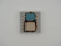
Weighing in at exactly 26.0 grams, this artifact feels like a solid block of industrial purpose. The high-fidelity micro-contrast captured in these macro shots is exceptional, allowing us to easily read the faint laser etching on the brushed metallic heat spreader without struggling against glare. It is a gorgeous, understated finish.
Turning the chip over reveals a pristine Ceramic Ball Grid Array. The ceramic substrate has that classic, slightly muted tone characteristic of high-end server gear. The solder balls are perfectly uniform, indicating this piece was likely never reflowed or mounted to a production board.
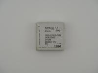
Here is the exact surface transcription from the heat spreader:
IBM MD [Circular M Logo]
0353     D53000GC
47P2622 ESD PQ
78629888-001
93BM     000107
This artifact utilizes a CBGA packaging technique. In the early 2000s, IBM heavily favored ceramic substrates for their enterprise silicon because organic packages simply could not handle the thermal expansion and dense pinouts required by their complex architectures. The ceramic material provides unmatched rigidity and thermal stability.
The thick, integrated metallic heat spreader was absolutely necessary. Chips of this footprint from IBM were notorious for running incredibly hot, demanding substantial airflow and heavy extruded aluminum or copper heatsinks. The densely packed ball grid array on the underside allows for massive I/O bandwidth, which was a critical requirement for memory controllers, storage interfaces, and crossbar switches in enterprise environments.
During the late 1990s and early 2000s, IBM's Microelectronics Division (noted by the "MD" on the surface) was a global titan of silicon fabrication. They were not just making central processing units. They were churning out highly specialized Application-Specific Integrated Circuits (ASICs) that powered the global financial system, massive database servers, and even consumer game consoles.
There is a common misconception that every large piece of ceramic IBM silicon from this era is a central processor. In reality, modern computing architectures require a symphony of support chips. A single IBM pSeries server might feature two actual CPUs but a dozen massive ASICs handling memory routing, I/O offloading, and cache coherency. These unsung heroes of the motherboard did the heavy lifting that allowed the flagship CPUs to shine.
This specific unit presents a fascinating forensic challenge. Lacking a prominent marketing name like "POWER4", we have to decode the nomenclature like hardware detectives.
I am highly confident this is a custom ASIC destined for an enterprise server, rather than a central processing unit. The 0353 string is a classic date code pointing to the 53rd week of 2003. The 93BM string is a critical clue. "BM" almost universally designates IBM's Bromont fabrication and packaging facility in Quebec, Canada. Bromont has historically been IBM's premier site for advanced ceramic packaging and flip-chip assembly.
The primary part number, 47P2622, aligns perfectly with IBM's Field Replaceable Unit (FRU) and internal part numbering schemes for system board components used in their eServer, xSeries, or pSeries machines of that era. The D53000GC is likely an internal engineering or batch identifier. Given the size and pin density, my educated guess is that this artifact served as an advanced memory controller or a high-speed PCI-X bridge chip. While we may not have the exact motherboard schematic to pin it down today, the physical evidence clearly points to a high-bandwidth enterprise application.