Weighing in at exactly 2958.0 grams, nearly three kilograms of heavy metals, aerospace-grade engineering, and pure computing. Far exceeding the footprint of a standard 2-inch package, this massive glass-ceramic MCM (Multi-Chip Module) is a monument to an era when physical scale equated directly to computational dominance.
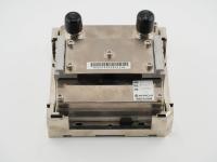
The top housing features a thick, machined metal block secured with precisely torqued hex bolts. The two large, black-capped nozzles on opposing corners are the fluid inlet and outlet ports. In the center sits a raised black sub-module featuring a single amber LED indicator with a pristine white label reading CONCURRENT MAINTENANCE READY. This detail highlights the high-availability nature of the MP5800, allowing operators to know exactly when it was safe to pull or service the unit while the rest of the massive frame stayed online.
Transcribing the primary identification sticker on the top plate, we get:
HDM     XSH01-B
REV.    J (A1)
SER.    67SC33
        001
HITACHI
MADE IN JAPAN
There is also a separate barcode sticker reading *02967SC33001W*.
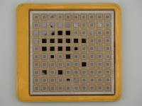
Flipping this massive block over reveals the true beauty of high-end mainframe packaging. The bottom is a vast, flawless expanse of white ceramic, completely covered by a meticulously organized sea of gold pins. The micro-contrast on the ceramic edges reveals extremely faint, precise laser etchings. Scanning the perimeter, we can clearly read:
HITACHI MADE IN JAPAN M02-2 HDXS-1 482
XSH01-B
BDREV-0
XSH01-BJ
To understand the engineering here, we have to look at the transition of logic gates in the mid-1990s. The Skyline MP5800 utilized "Advanced CMOS-ECL" (ACE) technology. While it incorporated CMOS to save power where possible, the heavy lifting and raw speed relied heavily on Emitter-Coupled Logic (ECL).
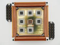
By utilizing a multi-chip carrier approach, Hitachi could mount dozens of bare silicon dies directly onto that single, massive ceramic substrate. The ceramic acts as an incredibly complex, multi-layered printed circuit board, routing thousands of microscopic electrical pathways between the chips. However, packing that much high-speed logic (likely Emitter-Coupled Logic or early high-power BiCMOS) into a dense cluster generates an apocalyptic amount of heat.
Packing that much high-speed ECL logic into a dense cluster generates an apocalyptic amount of heat. This is why the top of the module is dominated by that heavy metal plumbing block. Chilled water was pumped continuously through those capped ports, flowing through internal channels to pull heat directly away from the silicon dies via spring-loaded thermal pistons or highly conductive thermal paste. The proprietary PGA interface consists of thousands of delicate gold pins brazed onto the ceramic. Inserting this into the MP5800 backplane required specialized mechanical locking levers; human hands simply cannot apply the uniform force needed to seat thousands of pins simultaneously without bending them.
The story of this chip is the climax of the fierce, high-stakes world of Plug-Compatible Mainframes. For decades, Japanese technology giants like Hitachi built massive iron that executed IBM's proprietary instruction sets natively, often running faster than IBM's own hardware.
The Hitachi MP5800 Skyline represents the absolute zenith and the swan song of water-cooled, ECL-based mainframe engineering. Hitachi poured billions into materials science to match and exceed IBM's thermal conduction modules. When IBM pivoted to strictly air-cooled CMOS in the mid-90s, Hitachi released the Skyline as the ultimate powerhouse, brute-forcing performance with massive liquid-cooled modules before they, too, were forced to transition to pure, cooler-running CMOS architectures with the subsequent MP5600 series.
Identifying the exact machine this module was pulled from requires a bit of forensic deduction. The heavy metal flight case provides our best starting clue with the bold IP/IC TYPE stencil. In mainframe architecture, "IP" almost universally stands for Instruction Processor. This tells us we are looking at the core computational heart of the system, not a channel controller or a storage director.
The prefix HDM on the main label likely stands for Hitachi Data Module. Given the presence of the CONCURRENT MAINTENANCE READY indicator and the liquid cooling ports, this piece dates back to the era of massive ECL or early CMOS hybrid mainframes. The proprietary PGA and the liquid cooling strongly align with the Hitachi EX series or the legendary Hitachi Skyline series from the mid-to-late 1990s. The Skyline systems were famous for being the last, greatest gasp of water-cooled bipolar mainframe architectures before the industry shifted entirely to air-cooled CMOS.
While we cannot definitively pinpoint if this XSH01-B is the primary instruction processor for a Skyline or an earlier MP-series frame without access to restricted Hitachi field service manuals, the physical evidence is prevalent. The sheer weight, the liquid plumbing, and the thousands of gold pins confirm this is a top-tier, enterprise-class instruction processor module built to rival the biggest machines on the planet.
For an archival exhibit, this artifact is a centerpiece. The MADE IN JAPAN stamp represents a period of intense national pride in precision manufacturing. Presenting this module involves highlighting the sheer contrast between the brutalist, industrial plumbing on the top and the delicate, immaculate gold-and-ceramic artwork on the bottom. It is a flawless representation of peak 1990s supercomputing architecture.