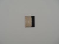
Here we have a particularly mysterious piece from the vault. This specific unit is not a retail processor, nor is it a standard engineering sample meant for benchmark leaks. It is a strictly internal NVIDIA test vehicle. When setting this artifact on the digital scale, it weighs in at a hefty 36.9 grams. That mass comes almost entirely from the massive, nickel-plated copper integrated heat spreader (IHS) and the thick organic substrate.
The laser etching on the matte metallic surface read:
NVIDIA (Logo)
33N3X9 .1133A1
A   TAIWAN
N4R526.M0P
TEST SAMPLE 3
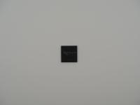
The physical textures are fascinating. The IHS has a distinct, slightly porous matte finish typical of pre-production or industrial-grade components, lacking the high-polish sheen of consumer retail silicon. Flipping the chip over reveals a high-density Ball Grid Array (BGA). The solder balls are perfectly intact and arranged in a thick perimeter grid, leaving a perfectly square, unpopulated void in the center of the green fiberglass PCB. The brazing and general assembly quality are top-tier, confirming this was manufactured on the exact same assembly lines as live silicon.
To understand a piece like "TEST SAMPLE 3", you have to step away from clock speeds and transistor counts and think about the physical realities of hardware manufacturing. This chip likely contains no functional logic. Instead, it is a mechanical and thermal dummy.
When board partners (like ASUS, EVGA, or MSI) design custom cooler shrouds, massive heatpipes, or complex vapor chambers, they cannot use $500 live silicon to test their mounting pressure. If a heatsink is screwed down too tightly, it will crack the die or warp the substrate. This test sample exists to take that abuse. It provides the exact physical dimensions, the exact thermal mass, and the exact package stiffness of the final product.
Engineers use these vehicles to calibrate pick-and-place machines on the factory floor, ensuring the robotic arms apply the correct amount of force when dropping the chip onto a freshly pasted motherboard. They also use them in thermal chambers, often with embedded thermocouples, to map out heat dissipation before the real architecture ever boots up.
The year 2011 was a wildly volatile era for NVIDIA. They were coming off the incredibly hot and power-hungry Fermi architecture (the infamous GTX 400 and 500 series) and were desperately working on the efficiency improvements that would become Kepler (the GTX 600 series).
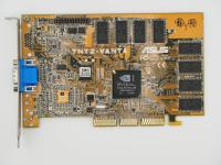
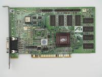
The lore surrounding these test samples is that they are the unsung heroes of the "Heavy Metal" hardware era. Back then, GPU coolers were getting absurdly massive. We were transitioning from single-slot blower fans to triple-slot aluminum monoliths. The sheer weight hanging off the PCB was enough to cause structural failure. Test samples like this one were sent down into the trenches to ensure that a two-pound block of copper and aluminum would not shear the BGA solder balls clean off the board during shipping.
Because this is internal test silicon, there are no public whitepapers or datasheets for "N4R526.M0P". However, we can forensic this quite accurately.
The date code 1133A1 is our biggest clue. This translates to the 33rd week of 2011, which places its fabrication right in the middle of August 2011. Using the ruler in the archive photographs, the package measures approximately 38mm by 38mm. This specific square footprint and IHS style strongly align with NVIDIA's desktop graphics processors of that period.
Given the mid-2011 timeline, this physical package was likely a test vehicle for the late-stage Fermi refresh or the early mechanical prototyping for the GK104 (Kepler) silicon which launched in early 2012. It is highly probable that this exact physical layout was used by third-party cooler manufacturers to design the thermal solutions that defined the 2012 GPU market. It is a brilliant, heavy piece of industrial history that survived the scrap bin.