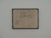
There is no heavy ceramic or intricate gold brazing here. Instead, we have a standard organic fiberglass substrate and a stamped copper Integrated Heat Spreader plated in nickel.
The text is sharp and perfectly legible against the slightly matte finish of the metal. Here is the exact transcription of the surface data:
AMD Ryzen 3 1200
AMD RYZEN
YD1200BBM4KAE
UA 1724SUS
9GW9549R70100
DIFFUSED IN USA
MADE IN CHINA
© 2016 AMD
Flipping this artifact over reveals the classic AMD Pin Grid Array. The PGA-1331 layout is dense. The gold-plated pins are pristine on this specific unit. You can clearly see the central square void and the corner keying missing pins that define the AM4 socket orientation. It is a very clean, flawless example of modern consumer silicon.
This chip represents the absolute foundational building block of the Summit Ridge family. The Zen architecture was a massive departure from the failed Clustered Multithreading approach of the Bulldozer era.
Underneath the IHS lies a single 14nm FinFET die fabricated by GlobalFoundries at Fab 8 in New York. The DIFFUSED IN USA text explicitly confirms this origin, while the final packaging and pin attachment occurred in Suzhou, China. The die itself packs 4.8 billion transistors into a 213 square millimeter area.
The engineering quirk of the Ryzen 3 1200 is its internal configuration. AMD built Summit Ridge using Core Complex (CCX) modules containing four cores each. To create this entry-level quad-core chip, AMD did not just use a single CCX. Instead, they utilized a 2+2 configuration across two distinct CCX units, disabling two cores per complex to improve yield on dies with minor defects. Furthermore, Simultaneous Multithreading (SMT) was fused off, leaving this processor with a strict 4-core, 4-thread limit. Running at a base clock of 3.1 GHz with a modest 65W Thermal Design Power, thermal management for this silicon was practically an afterthought. It runs exceptionally cool.
To understand the prestige of the Zen architecture, you have to remember the dark ages of AMD. Prior to 2017, Intel held a brutal, unyielding monopoly on the desktop and server markets. AMD was bleeding cash, and their processors were largely considered hot, inefficient afterthoughts.
Zen changed everything. It brought a massive 52 percent increase in Instructions Per Clock over the previous Excavator architecture. While the flagship Ryzen 7 1800X stole the headlines, the Ryzen 3 1200 was the unsung hero for the masses. Released in July 2017, it democratized true quad-core performance.
The best lore surrounding this specific model was its overclocking headroom. Because AMD unlocked the multipliers on all Ryzen processors, a budget builder could drop this $109 chip into a cheap B350 motherboard and crank the clockspeed past 3.8 GHz using the stock cooler. It completely cannibalized Intel's locked Core i3 lineup at the time. It is not a rare chip, but it is a highly respected working-class hero in CPU history.
The forensic identification is definitive based on the laser-etched OPN (Ordering Part Number).
The code YD1200BBM4KAE breaks down perfectly according to AMD's internal nomenclature:
YD: Ryzen brand for desktop.1200: Model number.BB: 65W TDP.M4: AM4 socket.K: 4 cores.AE: Summit Ridge B1 stepping.Furthermore, the date code 1724SUS tells me exactly when this silicon was born. It was manufactured in the 24th week of 2017. The SUS suffix indicates assembly in Suzhou. The copyright date of 2016 simply denotes the year the Zen architecture intellectual property was registered, not the manufacturing date. Everything aligns perfectly with a retail boxed unit from the early launch window.