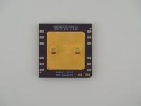
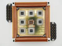
A standard bare VR4400 die or even a typical desktop PGA package is much smaller. What I have here is not just the processor. This is a complete Multi-Chip Module (MCM) containing both the VR4400MC processor and its entire secondary cache array, unified on one brutalist slab of purple ceramic.
Holding this specific unit in my hand, the sheer density of 1990s "big iron" engineering is immediately apparent. Tipping the scales at a hefty 84.7 grams, this artifact feels more like a weapon than a processor. It lacks the massive, imposing footprint of an IBM Thermal Conduction Module, but it shares that same uncompromising, heavy-metal design philosophy that I absolutely live for.
Here is the exact surface text transcribed from the artifact:
Top Side SRAM Modules (x9):SONY JAPAN
CXK5818120TM
-11
613A19EZ
Bottom Side Gold Lid:NEC JAPAN
MR-4401A-200
960914ES3.0
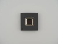
The construction is fascinating. On the bottom, we have a pristine gold-plated circular lid brazed onto the ceramic, protecting the main CPU die. Surrounding it is a dense, staggered pin grid array with specific keep-out zones populated by tiny surface-mount decoupling capacitors. Flipping the artifact over reveals a beautifully brutalist multi-chip module layout. Nine Sony synchronous SRAM chips surround a machined aluminum standoff block block block. This block is drilled and threaded, clearly serving as the structural mounting point for a massive external heatsink that would have clamped down over the entire assembly.
This artifact is an NEC-fabricated VR4400MC processor, which is a localized manufacturing spin of the legendary MIPS R4400 architecture. The MC designation signifies that this is a multiprocessor-capable variant, designed to be deployed in massive symmetric multiprocessing systems.
The engineering of the package itself tells a story of thermal struggle and memory bandwidth starvation. The primary R4400 die under the gold lid is a superscalar 64-bit powerhouse. However, feeding that pipeline required incredibly fast data access. The nine Sony CXK5818120TM chips on the top act as the external Level 2 cache. Having nine chips is a dead giveaway for error-correcting code memory (eight chips for data, one chip for parity/ECC). The "-11" suffix on the Sony memory indicates an 11-nanosecond access time, which was bleeding-edge for the mid-1990s.
Running at 200 MHz, this specific unit would have generated a significant heat load. The ceramic package is highly thermally conductive by design. The central aluminum block is not a heatsink itself. Instead, it is a structural anchor. A massive finned aluminum or copper heatsink would be screwed directly into those two threaded holes, applying immense pressure against the top of the SRAM chips and drawing heat through the ceramic from the die underneath.
My software engineering days at SIT never prepared me for the raw physical presence of this era of hardware. In the 1990s, MIPS was the absolute king of the workstation hill. When you think of the CGI revolution, the rendering of the dinosaurs in Jurassic Park, or the creation of the Nintendo 64 games, you are thinking of MIPS R-series processors doing the heavy lifting inside Silicon Graphics (SGI) workstations.
This specific module form factor was heavily utilized in SGI's legendary machines like the Indigo2 and the Challenge servers. There is a common myth that RISC processors of this era ran cool because of their streamlined instruction sets. This artifact proves that myth wrong. The R4400 was a beast, and it demanded heavy, expensive packaging to keep it stable. The sheer cost of fabricating a dual-sided ceramic multi-chip module with gold brazing and integrated cache memory was astronomical, restricting these chips strictly to defense contractors, high-end film studios, and academic supercomputing labs.
The most intriguing aspect of this specific unit is the laser etching on the gold lid: 960914ES3.0.
I have examined dozens of NEC and Toshiba MIPS chips, and standard production retail units generally feature a clean date code and a standard stepping revision. The "ES" suffix almost universally stands for Engineering Sample. The "3.0" likely indicates a third major stepping or revision of the silicon before final mass-market validation. The "9609" prefix suggests a date code of the 9th week of 1996.
This makes the artifact exceptionally rare. Engineering samples of workstation-class silicon were tightly controlled by SGI and NEC. They were typically loaned to major software developers or internal validation teams and were slated for destruction after the testing phase. Finding one that escaped the crusher and survived in this pristine condition is remarkable. While I cannot absolutely confirm which specific lab this unit was deployed in, the ES marking and the immaculate state of the PGA pins suggest it was likely pulled from a validation board rather than a production SGI Indigo2 case. It is a stunning piece of 64-bit history.