Holding this artifact in the hand is an absolute lesson in density. At a total weight of 161.7 grams with the heavy stainless steel retention frame attached, it feels less like a piece of computing equipment and more like an industrial weapon. When separated from the steel frame, the bare ceramic alone still registers a massive 72.4 grams on the scale.
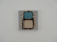
The physical construction is breathtaking. We are looking at a highly complex Land Grid Array package consisting of three massive exposed silicon dies mounted on a thick, dark reddish-brown ceramic substrate.
Edge Stamps: FR392629 FV730481
VPD EEPROMs: U3 A151Z
The central rectangular die is the primary processor, polished to a perfect mirror finish. It is flanked by two identical, perfectly square cache dies that exhibit a distinct, striking pinkish-purple hue under studio lighting. The bottom of the substrate is a vast sea of flawlessly brazed gold LGA pads designed to handle massive current delivery. There are no fragile pins here. This chip was built to be clamped down with immense mechanical pressure into an enterprise server motherboard socket. The thermal paste residue around the edges of the dies tells the story of a unit that saw active duty in a high-thermal data center environment before arriving in the archive.
The engineering inside this ceramic package is a testament to raw, brute-force performance. The central POWER6+ die is fabricated on a 65nm Silicon-on-Insulator (SOI) process. IBM shocked the industry with the POWER6 architecture by reverting to in-order execution. Instead of relying on complex out-of-order scheduling like almost every other modern processor, IBM engineers designed the pipeline to simply run at an unbelievably high clock speed, targeting up to 5.0 GHz. The "Plus" revision introduced in late 2008 brought additional memory keys for enhanced logical partitioning (LPAR) and optimized power delivery, allowing for even tighter enterprise virtualization.
The two pink flanking dies are the massive off-chip L3 caches. Because the primary CPU die only contains 8MB of L2 cache (4MB per core), IBM engineered the MCM to include two discrete 32MB L3 cache chips directly on the same ceramic substrate. These cache dies communicate with the processor over an insanely wide 80 GB/s internal bus.
The thermal challenges of this design were immense. The heavy metal frame surrounding the ceramic is not just for structural integrity. It is engineered to evenly distribute the massive mounting pressure required for the LGA interface while absolutely preventing the ceramic from warping under extreme thermal cycling.
The lore surrounding the POWER6 and POWER6+ is steeped in architectural controversy. When IBM announced they were stepping backward from the out-of-order execution of the POWER5 to an in-order pipeline, the industry thought they had lost their minds. But the gamble paid off for specific enterprise workloads. By simplifying the pipeline, they could crank the clock speed into the stratosphere, making it a monster for single-threaded database transactions and massive AIX deployments.
There is also a fascinating visual crossover in this era of silicon. Because IBM fabricated the final generations of HP's proprietary processors (the PA-8800 and PA-8900) at the exact same East Fishkill facility, those HP chips share the same dark ceramic, the same pink SRAM dies, and the same edge lettering styles as this POWER6+. It is a constant trap for collectors, making verified artifacts like this one all the more valuable to the archive.
Cataloging bare ceramic enterprise chips is incredibly treacherous. You will find endless websites, auction listings, and e-waste sellers pasting the ultra-high-end IBM P595 8-core server specifications under photos of this exact 2-core module.
A thorough visual analysis proves the true identity of this piece. The legendary IBM P595 8-core MCM is a massive, completely different square board packed with eight dense silicon blocks. Looking at the high-fidelity images of this specific unit, the layout is clear: one central processor and exactly two flanking L3 caches. This layout is definitively the 2-Core POWER6+ MCM, the beating heart of mid-to-high-tier IBM enterprise machines. It stands as a beautiful, heavy, and historically significant piece of Big Blue silicon.