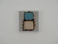
Measuring precisely 95mm by 95mm across, this is a monolithic slab of dense, multi-layered brown glass-ceramic. It was originally covered by a massive, hermetically sealed copper hat, but exposed like this, it is an absolute visual masterpiece of high-end silicon.
Looking at the side profile, the thick ceramic substrate features a distinct laser-etched serial number:
Edge Engraving: FY853673
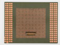
Flipping the module over reveals a breathtakingly dense Land Grid Array (LGA). The flat, gold-plated contact pads are arranged in four distinct quadrants. They show realistic, slightly matte surfacing consistent with a module that was once socketed under extreme mounting pressure.
Returning to the top, it is dominated by eight massive dies. The four central dies exhibit the muted, purplish-grey anti-reflective passivation typical of standard logic logic blocks. However, the four corner dies are what truly catch the light: they possess a brilliant, iridescent blue-green shift. This diffraction grating effect is the unmistakable visual signature of massive, highly repetitive SRAM cell arrays. A central metal standoff disc sits right in the middle, likely designed to prevent the heavy copper cooling cap from crushing the delicate dies, while hundreds of tiny, surface-mount decoupling capacitors tightly frame the silicon.
Diving into the technical weeds, this artifact is a masterclass in extreme computing density. This is an IBM POWER5 Multi-Chip Module (MCM).
To understand what we are looking at, we have to break down the die topology. The four central logic dies are the actual POWER5 microprocessors. Each of these chips contains two individual CPU cores, meaning this single ceramic package operates as an 8-way Symmetric Multiprocessing (SMP) super-node.
But IBM didn't stop at the logic cores. Those four corner dies are dedicated Level 3 (L3) Cache chips. Each one of those silicon slabs holds 36 Megabytes of SRAM. By physically moving the L3 cache off the processor die but keeping it on the same ceramic substrate, IBM achieved incredible yield rates while keeping memory latency impossibly low. The total module houses a staggering 144MB of L3 cache—an absurd amount of high-speed memory for 2004.
To wire all of this together, that brown glass-ceramic substrate contains 89 internal layers of microscopic routing. It shuttles data between the core dies, the cache dies, and the system bus at terrifying speeds. To feed this beast the necessary current and I/O bandwidth, the bottom of the module interfaces with the motherboard via exactly 5,183 LGA pads. When fully operational under enterprise loads, this 95mm square could draw over 800 watts, requiring aggressive liquid cooling or hurricane-force air impingement to keep the silicon from melting.
The POWER5 was a watershed moment in server architecture. Deployed primarily in IBM’s System p5 and System i5 enterprise servers, it was a brute-force answer to the escalating server wars of the mid-2000s.
One of the most significant legacies of this specific architecture is the introduction of Simultaneous Multithreading (SMT) to the POWER line. While Intel was pushing "Hyper-Threading" in desktop Pentium 4s, IBM engineered SMT from the ground up for massive database and transaction workloads. Each of the 8 physical cores on this MCM could execute two threads simultaneously, presenting 16 logical processors to the operating system.
The lore of these MCMs usually revolves around their physical dominance. At a time when x86 servers were struggling to scale past 2 or 4 sockets cleanly, IBM was dropping these 8-core, 144MB-cache monoliths onto motherboards. They were so powerful that single System p5 frames often replaced entire racks of competing Sun Microsystems or HP servers.
Identifying this piece leaves virtually no room for ambiguity; the physical footprint is an absolute fingerprint.
My immediate identification stems from the highly specific 8-die layout combined with the 95mm footprint. The predecessor to this chip, the POWER4 MCM, utilized an 89mm substrate and primarily housed just four processor dies. The successor, the POWER6, shifted topologies yet again.
This exact configuration, four central dual-core CPU dies surrounded in a diamond pattern by four massive L3 cache dies, is the definitive, exclusive hallmark of the fully populated POWER5 MCM. Furthermore, the 4-quadrant layout of the 5,183 LGA pads perfectly matches the proprietary socket IBM engineered for their mid-2000s enterprise frames. It is a spectacular, brutally engineered artifact from an era when IBM completely dominated the heavy-iron server market.