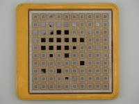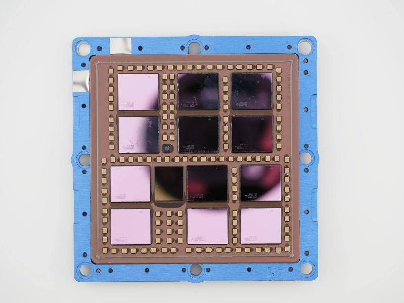
This isn't a standard, off-the-shelf processor; it is a monolithic, bare-die slab of high-end computing history. This came with a striking blue anodized aluminum frame simply as a protective tray to hold the module, though the "PARICON" label indicates it was originally manufactured as an elastomeric carrier designed to temporarily clamp the bare substrate into an LGA test socket for engineering validation.
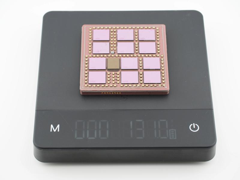
If we zoom in, the micro-contrast reveals a stunning layout: exactly 12 physically identical main dies arranged in a perfect grid, alongside a single, tiny clock/logic chip sitting just off-center. The dies feature a distinct, purplish anti-reflective passivation layer, which is a visual hallmark of IBM’s CMOS fabrication from the early-to-mid 2000s. The entire complex is perfectly framed by a dense perimeter of pristine golden surface-mount decoupling capacitors.
Carrier Label 1: 25007
Carrier Label 2: PARICON
Silicon Etching (Bottom Right Die): 2107409 IBM
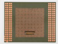
Diving into the technical weeds, the packaging of this module is an absolute masterclass in electrical engineering. IBM's glass-ceramic substrates are legendary for a reason. Because the thermal expansion coefficient of glass-ceramic closely matches that of the silicon dies, IBM could mount these chips directly to the substrate using C4 (Controlled Collapse Chip Connection) flip-chip bumps without tearing the fragile interconnects apart as the chips furiously heated up and cooled down under immense enterprise workloads.
Inside that thick, purple ceramic slab are dozens of layers of microscopic wiring, routing power, ground, and high-speed data between the twelve dies at latencies impossible to achieve on a standard fiberglass motherboard. What makes this specific PariPoser setup so vital to the engineering process is yield validation. Before IBM committed to permanently brazing thousands of gold-plated pins or spheres to the bottom of the MCM which is a highly expensive process, they would use these Paricon frames to temporarily socket the module, boot it up, and run exhaustive diagnostics to map any defects across the twelve nodes.
In the halls of hardware lore, IBM’s MCMs represent the ultimate philosophy of the mainframe era: keeping everything as physically close as possible to defeat the speed of light. While competitors were fighting over desktop sockets and front-side bus speeds, IBM was building localized superhighways inside single packages.
There is a common myth that all mainframe silicon was essentially the same as high-end server silicon, just packaged differently. This is patently false. Chips destined for these MCMs were engineered with massive amounts of proprietary I/O to talk directly to dedicated cache chips and system control dies. The architecture was designed from the ground up for extreme redundancy. The thermal density of tightly packing 12 identical high-performance dies onto a single substrate would have required an insanely aggressive cooling solution in a production environment.
Whenever I examine this piece, it serves as a humbling reminder that IBM's internal engineering labs produced hardware that completely defies standard public documentation.
For a long time, the 9S-SOI CMOS aesthetic and the mid-2000s era footprint made it incredibly tempting to classify this as a mid-range zSeries module, specifically a z890. However, a strict forensic analysis of the physical die layout absolutely shatters that assumption. A true IBM 2086 (z890) MCM has a very specific, hard-coded configuration: it provides support for exactly 5 PU (Processor Unit) dies sitting alongside its shared Level 2 cache.
This artifact has 12 perfectly identical, homogeneous dies. Furthermore, the gold decoupling capacitors tightly trace this 3x4 grid without any empty "voids" or unpopulated pads. This means the glass-ceramic substrate wasn't just a half-empty vessel for a larger machine like the z990 (which used 20 dies); it was purposefully and specifically engineered only to hold these 12 identical chips.
Because it is an engineering sample housed in a lab-exclusive Paricon test carrier, we are looking at a spectacular, undocumented prototype. It completely breaks the mold of standard zSeries topologies of its era. Whether it was a highly specialized test vehicle or an experimental node that never saw the light of a data center floor, it remains one of the greatest, most beautiful mysteries in the collection.