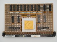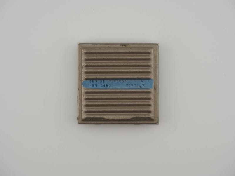
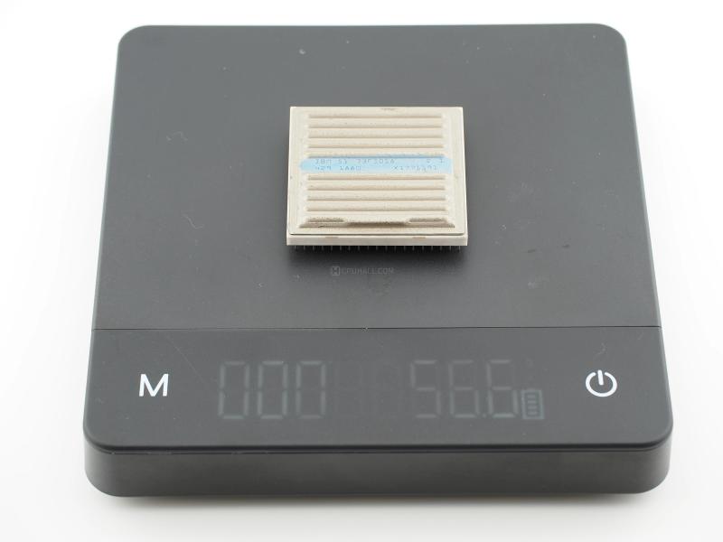
Holding this piece under the light, the sheer density of the engineering is immediately obvious. Clocking in at 56.6 grams for a module roughly 45mm across, it feels like a solid ingot of cold war era technology. Dropping it under my macro lens reveals a staggering level of manufacturing fidelity that modern organic substrates simply lack.
Here is the exact text stamped across the striking blue painted stripe on the finned heatsink:
IBM 51  73F5018          Q  1
429   1880       X1771191
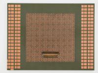
The contrast between the matte grey metal of the integrated heat spreader and the stark white alumina ceramic base is visually arresting. Flipping the module over, the PGA layout is mesmerizing. The pins are thick, heavily gold-plated, and individually brazed onto the ceramic package. You can clearly see four red circular standoff beads placed specifically on corner pins. These were designed to ensure the module sat at the exact correct height when wave-soldered or socketed into a massive planar board.
This artifact represents the absolute peak of late 1980s thermal and packaging engineering. IBM did not build consumer toys. They built iron. The cap you see on top is not just a heatsink. It is a hermetically sealed thermal enclosure, likely filled with a specialized thermal paste or inert gas to rapidly pull heat away from the bipolar logic die or gate array housed inside.
The ceramic substrate itself is a marvel. Before the era of cheap fiberglass PCBs, IBM utilized multi-layer alumina ceramic to route the incredibly complex web of connections from the silicon die down to the gold pins. This material was chosen because its coefficient of thermal expansion closely matched the silicon it hosted. This prevented the chip from literally tearing itself apart as it heated up and cooled down during the daily operational cycles of a mainframe environment. The finned aluminum cap maximizes surface area for the high-velocity chilled air that would have been screaming through the chassis of whatever system this came from.
There is a unique mystique surrounding IBM's proprietary silicon from this era. While the rest of the world was standardizing on x86 processors in plastic or cheap ceramic packages, IBM's Enterprise Systems division was operating in an entirely different universe. They designed their own fabrication nodes, wrote their own instruction sets, and engineered their own packaging.
A common myth among novice collectors is that any large, heavy IBM chip from this era is a legendary water-cooled Thermal Conduction Module. While those massive, multi-kilogram blocks of plumbing and helium certainly exist, the reality of mainframe architecture is that it required hundreds of these smaller, highly specialized support modules. This specific unit was the blue-collar worker of the mainframe world. It handled the crucial, invisible tasks like memory control, channel I/O routing, or cryptographic acceleration. It was designed to run flawlessly for decades without a single flipped bit.
Identifying exact IBM part numbers from the late 80s and early 90s is notoriously difficult. IBM tightly guarded their internal hardware documentation, reserving it strictly for their legendary "Customer Engineers" who serviced the machines in the field.
When researching the 73F5018 part number, I have to rely on educated deductions. The 73F prefix frequently appears in the parts catalogs for the IBM AS/400 midrange systems and the lower-end ES/9000 mainframe series introduced right around the late 1980s into the 1990s. The 1880 stamp is likely a date or plant code, and the X1771191 serves as a serialized batch or wafer identifier.
While I cannot definitively pinpoint whether this is a cache controller or a specific channel interface gate array without an original IBM field service manual, the physical evidence points firmly to it being a critical support IC. The dense PGA footprint and the aggressive thermal management solution prove it dissipated significant power, which is the hallmark of IBM's high-speed bipolar logic from the twilight years of the Cold War.