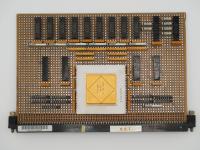
As verified on the scale, it sits at a dense 27.7 grams. This is not consumer-grade silicon. This is enterprise heavy metal. Measuring precisely at around four centimeters square, the unit features a flawless white ceramic substrate capped by a meticulously machined aluminum heat spreader.
When observing the top plate under directional light, the laser etching reveals its identity with crisp precision. Here is the raw surface transcription:
47P4605        PQ
IBM93      C250003V
1
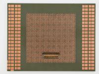
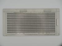
The micro-contrast of the text against the brushed metal is fantastic. Flipping this specific unit over reveals a stunning, fully populated Pin Grid Array. The sheer density of the pins is mesmerizing. There are no missing corners or empty zones. The brazing work connecting each pin to the ceramic base is a testament to the manufacturing standards of early 1990s enterprise hardware.
The engineering encapsulated in this package is a masterclass in thermal and electrical management. During this era, driving high-frequency signals across dense logic arrays required massive I/O capabilities. The pin density on the bottom of this CPGA form factor indicates a very wide data bus and significant power delivery requirements.
This is not just a chip. It is a highly specialized thermal conduction vessel. The aluminum cap is not merely decorative. It is bonded directly to the silicon die beneath it to spread heat rapidly before it even reaches a heatsink. Inside that thick white ceramic substrate, there are dozens of microscopic routing layers. IBM engineers had to perfectly balance signal integrity, power delivery, and thermal expansion coefficients so the ceramic would not crack under extreme enterprise workloads.
The year 1993 was a massive turning point for IBM. For decades, the company ruled the computing world with monstrous, water-cooled bipolar mainframes utilizing complex Thermal Conduction Modules. However, the early 1990s brought the CMOS revolution. IBM realized that to stay competitive, they had to transition their massive mainframe and high-end server architectures to smaller, cooler, and highly efficient CMOS designs.
Artifacts like this bridge that historical gap. It carries the physical heft and premium material choices of the old world, but it houses the highly integrated logic of the new world. A common myth in vintage computing circles is that all 1990s IBM chips were completely custom and isolated. In reality, chips from this era often shared underlying fabrication techniques across the S/390 mainframe lines and the AS/400 midrange systems. They are the unsung heroes that quietly ran the global banking and logistics sectors for a decade.
Identifying undocumented IBM silicon from the 1990s is always a thrilling forensic exercise. The markings on this piece give us excellent structural clues. The IBM93 stamping almost certainly indicates a mask copyright or fabrication baseline of 1993. The primary identifier, 47P4605, perfectly aligns with IBM's internal Field Replaceable Unit and part numbering schemes of that decade.
While I am constantly cross-referencing my archives, pinning down the exact system this was pulled from remains an educated hypothesis. The massive pin count and robust thermal cap strongly suggest this is a core processing element or a primary memory controller hub for a high-end RS/6000 or early CMOS S/390 mainframe node. The PQ marking likely denotes a specific fabrication plant or package qualification standard. Without the original system service manuals, the exact logic inside remains a beautifully sealed mystery. It stands as a prime example of transition-era IBM engineering.