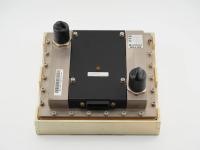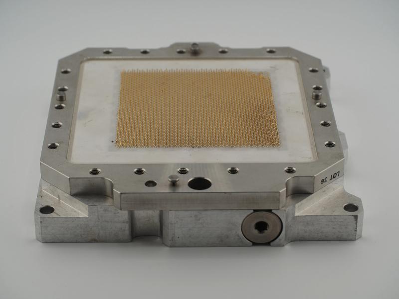

Handling this artifact is a physical event. Placing this specific unit on the scale reveals a staggering weight of exactly 1619.3g. We are talking about over 1.6 kilograms of computing history packed into a square block measuring roughly six inches across. The top hat is secured by heavy hex bolts that seal the internal environment.
Here is the exact transcription from the side label:
MCP   A5984301        ASM           P/N   53F0954
E.C.  C22849          IBM           PHASE
DATE  12MAY90                       JOB   YR1L1125
FIELD S/N 300X9807631               MADE IN JAPAN
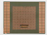
There is also a faint LOT 36 stamped into the metal housing on one of the chamfered corners, alongside some handwritten markings that look like TC-10... scribbled by an engineer decades ago. Setting this up under my Olympus E-P7, I had to dial in the macro lens just right to capture the staggering density of the gold pins on the bottom. It was a struggle to capture within the frame in my tiny product lightbox. The substrate is a brilliant white ceramic, and the pins are flawlessly brazed onto the surface (barring the unfortunate pin damage from handling).
The engineering inside this metal fortress borders on science fiction. The Thermal Conduction Module was IBM's extreme solution to a massive thermal problem. They were packing dozens of high-speed bipolar logic and memory chips onto a single multi-layer ceramic substrate. To get the heat out, the inside of this block is machined with individual spring-loaded aluminum pistons. Each piston makes direct physical contact with the back of a silicon die.
To maximize thermal transfer, the entire internal cavity was filled with helium gas because it conducts heat significantly better than air. The heat traveled up the pistons and into the massive metal cap, which was then bolted to a heavy water-cooling cold plate inside the mainframe chassis. The ceramic substrate itself is a masterpiece. It contains over thirty distinct layers of wiring pressed together and fired, routing signals between the chips and down to the thousands of gold pins on the bottom. This approach eliminated the signal delay of sending data across a traditional printed circuit board.
The IBM 3090 series was the absolute king of the data center in the late 1980s. When you withdrew cash from an ATM, processed a massive corporate payroll, or routed an airline ticket, you were almost certainly relying on an array of these heavy metal bricks. They were wildly expensive and required extensive plumbing to keep cool.
There is a running joke in vintage hardware circles about the sheer violence required to scrap these units. Because IBM leased these machines, they usually took them back at the end of their life cycles. To prevent the grey market from reselling the parts, IBM would literally put the mainframes through industrial shredders to reclaim the gold. This is why finding an intact, sealed TCM is a collector's dream. It survived the crusher.
Based on the date code of 12MAY90 and the exact physical footprint, this module aligns perfectly with a later-generation IBM 3090 installation. The MADE IN JAPAN designation on the label is a wonderful detail. IBM operated a massive, highly advanced manufacturing facility in Yasu, Japan, which was instrumental in developing and producing these complex ceramic substrates and packaging technologies during the 1980s and 1990s.
Visually, the pin grid density and the specific hex-bolt pattern on the hat differentiate it from the earlier 3081 modules. While the exact part number 53F0954 does not map to a publicly available service manual for a specific logic function, the MCP prefix suggests it is a Multi-Chip Package handling either core arithmetic logic or high-speed cache control for the central processor complex. It is a stunning, definitive piece of mainframe history.